SECDA: Efficient Hardware/Software Co-Design of FPGA-based DNN Accelerators for Edge Inference
I was fortunate to recently work on a paper on hardware design, led by the talented Jude Haris. SECDA was published in October 2021, in the IEEE 33rd International Symposium on Computer Architecture and High Performance Computing (SBAC-PAD) conference. It was hosted in sunny Belo Horizonte, Brazil; but unfortunately we had to attend remotely due ongoing international travel difficulties.
The work discusses a co-design methodology we developed for efficiently producing FPGA accelerators. You can read the full paper here on arXiv, the following post just gives a brief accessible summary.
Background and Motivation
Hardware design is a complex field, and certainly one that I did not have much experience with before collaborating on this project. Hardware Description Languages (HDLs) allow one to define the logic of a computer hardware design using a programming language. This “hardware code” can then be followed as a recipe to be turned into real hardware. Low-level HDLs can be very verbose and hard to debug, see below the Verilog code for a “full adder”, which is a very low-level and relatively simple component, from the ECE232: Hardware Organization and Design course. Imagine having to write and debug 100,000 lines of code like this.
module FullAdder(a,b,cin,cout,sum);
    input a, b, cin;
    output cout, sum;
    wire w1, w2, w3, w4; // internal nets
    reg sum, cout; // registers retain value
    always @ (a or b or cin) //  Anytime a or b or cin CHANGE, run the process

    xor #(10) (w1, a, b); // delay time of 10 units
    xor #(10) (sum, w1, cin);
    and #(8) (w2, a, b);
    and #(8) (w3, a, cin);
    and #(8) (w4, b, cin);
    or #(10, 8)(cout, w2, w3, w4); // (rise time of 10, fall 8)
    end
endmodule
Similar to how few people write in assembly except for very specific optimisations, a range of higher level HDL paradigms have emerged, called high-level synthesis (HLS), which make it easier to more quickly design hardware.
However, what about how we actually build and test our hardware designs? We don’t all have an ASIC fab plant in our office. This is where FPGAs (Field-Programmable Gate Arrays) come in. FPGAs are reconfigurable circuits, which can take a representation of your hardware design, and change their internal dataflows to implement your circuit.
The process of turning a high-level hardware design into a circuit configuration on an FPGA is known as synthesis, and can take minutes to many hours, depending on the complexity of the design. Given how many different designs one will be tinkering with during a typical design process, this can translate to a large bottleneck. You could waste hours of your time sitting waiting to see the impact of your change.

A permissively licensed image of an FPGA - doesn’t look that interesting without decapping and a microscope (PoC||GTFO 4:9)
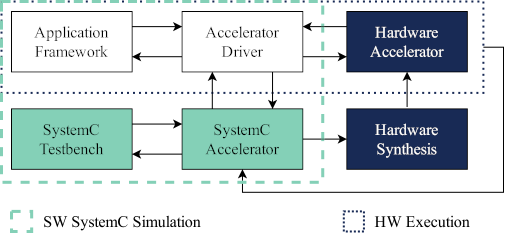
Different design methodologies (such as OpenCL and SMAUG) try to deal with the issue in different ways; which we compare and contrast in the full paper. However, we believe that our new design methodology SECDA (SystemC Enabled Co-design of DNN Accelerators) makes the right trade-offs, by making it cheap to evaluate new designs in a simulation, while having an easy path to hardware synthesis.
SECDA
SECDA attempts to solve these problems by simulating how the hardware will behave using the SystemC simulation framework which allows low cost software evaluation of hardware behaviour. However, unlike some other methods such as SMAUG, the SystemC definition of the hardware is also synthesisable to real hardware. This means that we can get data on parts of the system not modelled well in simulation (e.g. the memory inter-connect between the CPU and the accelerator), without having to run synthesis for every minor design change.
The low-cost SystemC simulation means that we can explore many more hardware design iterations, while still having the option of getting real hardware performance metrics. Additionally, the design of the SECDA methodology encourages the principles of hardware software co-design and co-verification. This is due to the fact that SECDA designs and integrates the software driver which bridges the application framework (the CPU-side code) and the hardware accelerator from the start. This allows designers to explore the trade-offs inherent in managing data transfer to-and-from the accelerator, which often becomes the bottleneck for optimised accelerator designs.
Overview of the SECDA design methodology
Case study
We evaluate the usability of the SECDA design methodology by designing two GEMM accelerators for quantised neural networks, integrated with the TFLite neural network inference framework.
You can see below our runtime model, with the GEMM driver being our software bridge between TFLite (via the Gemmlowp library), and our accelerator designs.
 Runtime model
Our two accelerator designs had some components in common, but followed two different data flows. The first accelerator is called “Vector-MAC”, and the second accelerator design is a systolic array design, which is a similar architecture to Google’s TPU. We evaluated three common neural networks using our accelerator designs, and improved significantly compared to using CPU-only inference in all cased - both in terms of reduced inference time and energy consumption.
For more details on these designs, how SECDA helped us gain insights into how to improve them, and their performance in terms of inference time and energy consumption, please refer to the full paper.
 Vector MAC design
 Systolic Array design
Conclusion
SECDA is my first published piece of work in the area of hardware design (as a co-author), and it really helped me understand some of the challenges and opportunities in this space. My main research focus right now is from the perspective of compilers for neural networs, and I really look forward to working more with Jude, and hardware experts like him in this Golden Age of Compiler Design in an Era of HW/SW Co-design.